A material such as graphene, representing a two-dimensional carbon lattice with a thickness of only 1 atom, has recently become increasingly popular. And study its properties by specialists from around the world. Just recently a group of researchers from the University of Melbourne for the first time managed to obtain images depicting the movement of electrons in the environment of this material. Early study of this process was impeded by several limitations. Understanding of the behavior of electrons in such conditions may give impetus to the development of electronic devices of new generation.
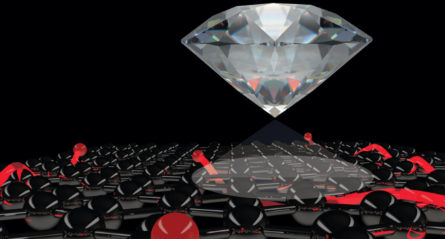
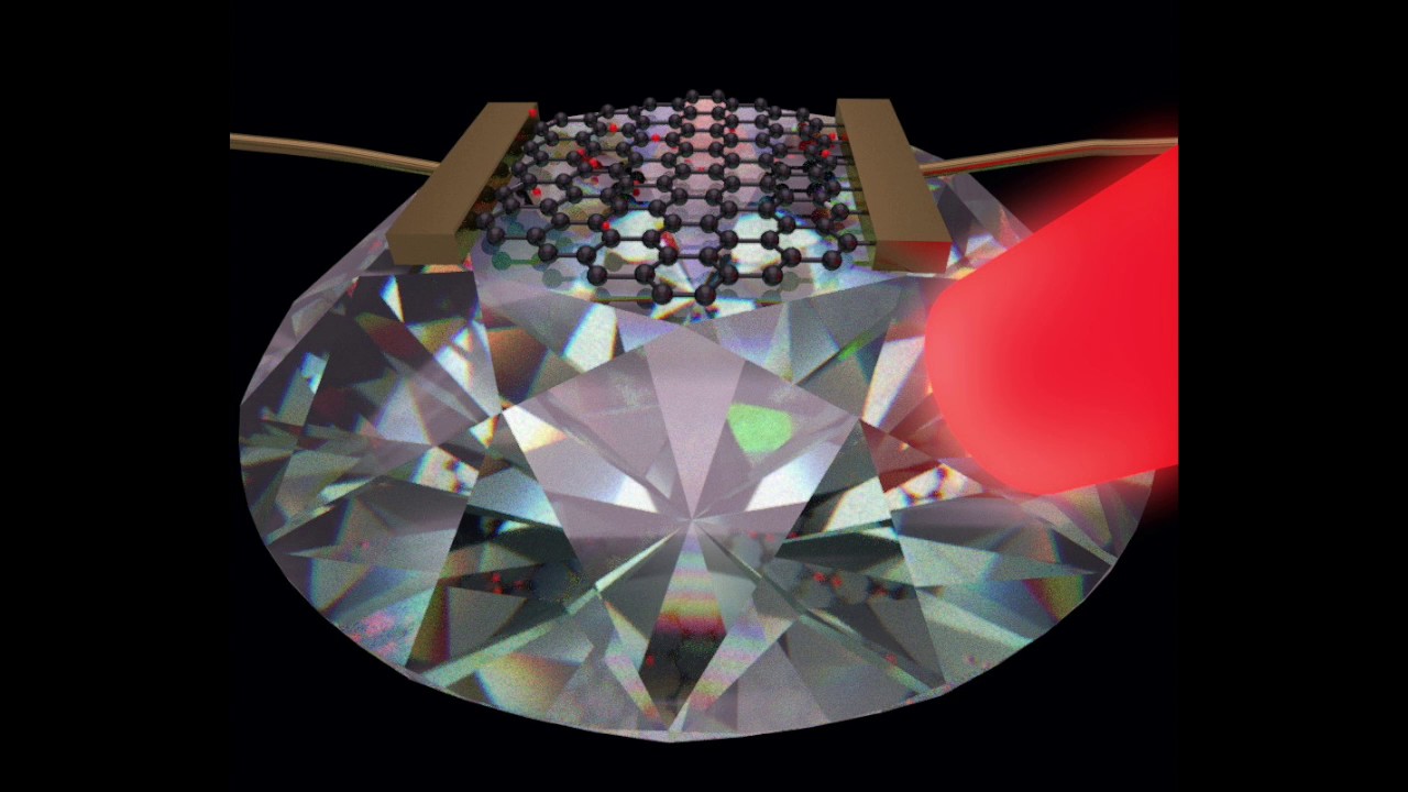
To pictures managed the research team, led by head of the Centre for quantum computation and communication technology Professor Lloyd Hollenberg. Scientists in the course of their research used quantum probe, the surface of which was created “colored spots”. They represent a kind of “free space” for the nitrogen atoms in the crystal lattice, where they moved during the reaction. The probe itself was made of diamond. According to the scientists,
“We were covering the diamond light green laser, and a “color stain” was bright red, the parameters of which depended on the interaction of nitrogen vacancies in diamond with electrons that moved in the environment of graphene. Changing the intensity of the red light, we carried out the measurement of a magnetic field generated by the movement of electric current. The equipment thus allows us to see not only the features of electron motion, but also to determine the magnitude of the impact on it of the defects present in the material”.
The experts themselves say that the developed technology will provide an opportunity to study peculiarities of the interaction of electric current not only graphene, but also with many other two-dimensional and ultra-thin materials. The study of their properties will allow to develop new types of electronic devices, solar panels and circuit boards.
“The production of electronic devices of the next generation who are likely to be based on ultra-thin and two-dimensional materials, faced with the complexities associated with small cracks and other defects. These defects will affect the motion of electrons whose behavior in thin materials is much different from what we have seen in conventional conductors”.
Scientists first managed to obtain images of electron motion in graphene
Vladimir Kuznetsov